


Semiconductor device analysis
We are also studying about application of SNDM for analysis of semiconductor devices. In this part, we show you principle of semiconductor measurement using SNDM and information that we can get using SNDM.
First, we review about semiconductor. There are many kinds of materials. When we focus on the electric conductivity, materials can categorized as
- metal
- semiconductor
- insulator
in order of conductivity. So, semiconductor is a material whose conductivity is less than that of metal but greater than that of insulator. The most important nature of semiconductor is variability of conductivity. This nature enables us to control electrons without depending on mechanical switches. Devices which control electronic flow by using semiconductors are called semiconductor devices. The most popular ones are diode and transistor. For functionality of semiconductor devices, n-type and p-type semiconductor are indispensable. The n-type semiconductor is semiconductor which contains many free electrons and whose electric conductivity is dominated by behavior of electrons. In contrast, p-type semiconductor has many holes and its electric conductivity is dominated by holes.
As you have seen, SNDM is a SPM which measures capacitance response to applied voltage.
Semiconductor can be a measurement target for SNDM, since the capacitance of semiconductor also depends on applied voltage.
We will consider the capacitor which consists of metal-electrode, oxide layer, and semiconductor, which is called MOS capacitor as illustrated in Fig. 1.
The capacitance C is given by following equation:
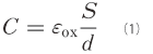
where εox, S, and d are dielectric constant of SiO2, thickness of SiO2 layer, and area of electrode, respectively.
As shown in Fig. 1, when positive external voltage is applied to the capacitor, a depletion layer is formed below the oxide layer, where the carriers are empty.
Since the depletion layer acts as insulator with the dielectric constant of Si, the capacitance C can be considered as series of two capacitors (oxide layer capacitor and depletion layer capacitor).
So the expression of the C is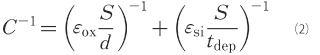
This equation represents that the capacitance C is reduced by depletion which is formed by applied voltage.
In other words, the capacitance depends on external voltage.
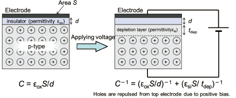
Fig. 1:MOS capacitor
The capacitance-voltage relationship mainly depends on the polarity of semiconductor (p- or n-type) and carrier density as Fig. 2 shows. When the MOS capacitor is constructed with n-type semiconductor, the capacitance is reduced by negative voltage since the carriers are negative charge. Next, we consider the effect of density. When the carrier density is low, depletion layer is easily formed by voltage, which results in strong voltage-dependence of capacitance (shown as solid line in Fig. 2). In contrast, MOS capacitance with high carrier density semiconductor has weak voltage-dependence (shown as dashed line in Fig. 2). If the carrier density is extremely high, the MOS capacitance equals to metal-insulator-metal capacitance and it has no voltage-dependence. As you see, measurement of capacitance-voltage (C-V) relationship gives us important information about semiconductor. If you want to know about C-V measurement in more detail, please refer to textbook of semiconductor or other websites.
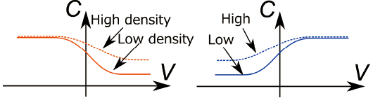
Fig. 2: Typical C-V curves
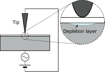
Fig. 3: Local C-V measurement with sharp conductive tip
When the electrode of MOS capacitor is replaced with sharp conductive tip, local C-V property can be measured and distribution of parameters about semiconductor can be mapped. In semiconductor measurement using SNDM, derivative of C-V (∂C/∂V), which depends on polarity and density of carrier, is acquired. By mapping of ∂C/∂V, SNDM visualizes distribution of carrier in semiconductor sample.
Following themes are main research about semiconductor in our laboratory:
- measurement of carrier distribution in semiconductor devices
- measurement of stored charge distribution in Flash memory
- carrier distribution imaging of SiC semiconductor devices
- measurement of two-dimensional electron gas (2DEG)
- measurement of monocrystalline Si solar cells
- super-higher-order SNDM
- Local-deep-level transient spectroscopy for investigation of MOS interface traps
- Time-resolved SNDM (Tr-SNDM)
- Nanoscale carrier distribution imaging on atomically-thin (two-dimensional) semiconductors
Measurement of carrier distribution in semiconductor devices
The carrier distribution is critical to performance of semiconductor devices. So it is important to measure the carrier distribution in fabricated devices. SNDM is powerful technique for this purpose. By scanning cross-section of the device as illustrated in Fig. 4, SNDM visualizes the cross-sectional carrier distribution. Figure 5 is result of cross-sectional measurement of FET whose gate length is 40 nm. Bright and dark area represent p- and n-type region, respectively. As you see, carrier distribution of very small device is clearly visualized.
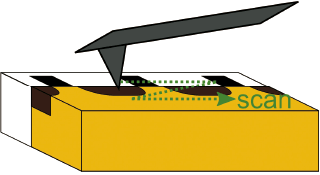
Fig. 4:
Overview of cross-sectional carrier distribution measurement
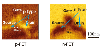
Fig. 5: Cross-sectional SNDM image of FET [1].
Measurement of stored charge distribution in Flash memory
As another application of SNDM for semiconductor device measurement, measurement of stored charge distribution in Flash memory was demonstrated. Flash memory is one of the widely used non-volatile memory device. Flash memory memorizes information by storing charges in floating gate or dielectric layer. In this measurement, MONOS flash memory, which stores charges in dielectric layer, was measured. Unlike the carrier distribution measurement, top face of device (not cross-section) was scanned as illustrated in Fig. 6. Figure 7 shows result of this measurement. Figure 7(a) is the image of a memory cell with no stored charge. Figure 7(b) and (c) are the images of memory cells where positive charges and negative charges are stored, respectively. The stored charges are well imaged and its polarity can be distinguished. This stored-charge-dependence of image contrast is caused by variation of effective bias. The stored charges change the electric field which is applied to semiconductor. Therefore, the charges change C-V property, which results in different contrast.
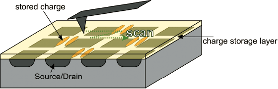
Fig. 6: Overview of stored charge distribution measurement
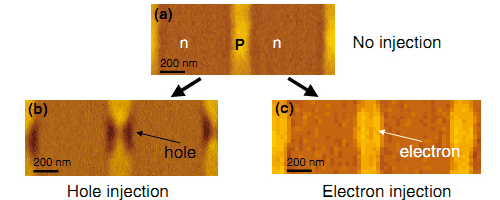
Fig. 7: Stored charge distribution in MONOS flash memory
Carrier distribution imaging of SiC semiconductor devices
SiC semiconductor devices are also measurement target of SNDM. Typical examples are shown in this section. Figure 8 is a SNDM image of cross-sectioned Vertical SiC-MOSFET.
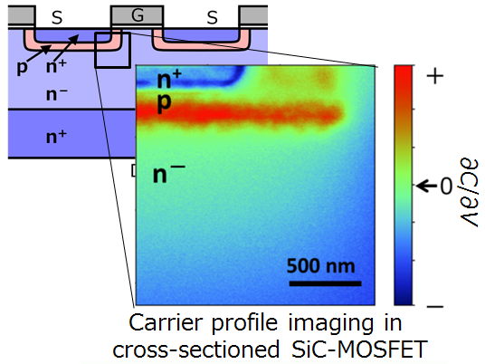
Fig. 8: A SNDM image of cross-sectioned SiC-MOSFET
Operated devices can be also measured. In following example, gate-source bias (VGS) dependent carrier distribution was measured by SNDM.
Fig. 9: The red box is region of interest.
Fig. 10: The obtained movie of VGS dependent carrier distribution.
Figure 9 indicates the measured area. Figure 10 was taken with AC VGS (about 100 Hz) beeing applied. In Fig. 10, red and green areas show p-type and n-type area, respectively. The VGS is desplayed at the left-top of the Fig. 10. We can see that the carrier distribution changes dependent on the VGS. Althoug channel formation (i.e., turn-on) is not imaged in this result, another result which visualizes channel formation is available on Ref. 2.
Measurement of two-dimensional electron gas
Wide-bandgap semiconductors are expected to become widely used new materials for power electronics devices. Compared to Si, GaN has a bandgap that is roughly three times larger, a breakdown field more than ten times higher, and an electron saturation velocity more than twice as large. Therefore, a GaN power device has low on-resistance and high-frequency operation characteristics. In particular, the AlGaN/GaN high-electron mobility transistor (HEMT) is a promising candidate as a high-power, high-frequency transistor. The main feature of the AlGaN/GaN heterostructure is that a two-dimensional electron gas (2DEG) is induced by spontaneous piezoelectric polarizations in AlGaN and GaN without doping. 2DEG is unaffected by impurity ionization scattering due to the dopant, so the device can maintain high electron mobility. There is much research on the high-performance AlGaN/GaN heterostructure. The 2DEG formation process has been investigated experimentally and theoretically. The thickness of 2DEG is calculated from its band structure. Such research shows that 2DEG is distributed within a range of 5-10 nm. Although local characterization is necessary for the effective development and improvement of device performance, there are a few experimental studies on the local characterization of the AlGaN/GaN heterostructure. SNDM is suitable for characterizing the AlGaN/GaN heterostructure because SNDM can be used to analyze both polarization in dielectric materials and carrier distribution in semiconductor devices with a high S/N ratio. Since the capacitance variation as a function of ac applied bias voltage reflects both carrier and polarization properties, SNDM can characterize both. In this work, we measure the cross-section of the AlGaN/GaN heterostructure and characterize the polarization and 2DEG by using SNDM.
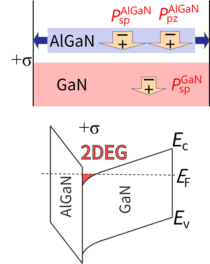
Fig. 11: Schematic band diagram of AlGaN/GaN heterostructure. EC, EV, and EF are the conduction band edge, valence band edge, and Fermi level, respectively. +σ is a positive polarization sheet charge induced by the discontinuity of polarizations at the AlGaN/GaN interface.
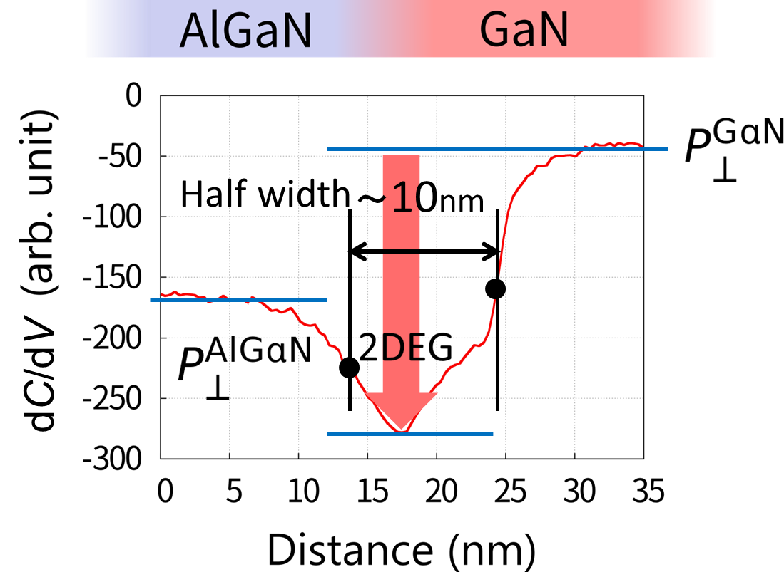
Fig. 12: Profiles of SNDM signal of AlGaN/GaN heterostructure measured by SNDM.
Measurement of monocrystalline Si solar cells
The performance of Si solar cells is dependent on the active dopant distribution in the emitter. Estimation of the dopant distribution in a Si solar cell is difficult owing to the pyramidal surface texture of the emitter. Here, we investigate the active dopant (carrier) distribution in a phosphorus (P)-implanted Si solar cell using SNDM. SNDM (dC/dV) and dC/dz-SNDM are complementarily applied to visualize the carrier distribution in a cross section of the Si solar cell. The carrier density in the emitter is calibrated using SNDM data taken from standard Si samples. The standard samples were measured by SNDM after SNDM measurements of the solar cell. Figure 13(a) shows the calibration curves, which show the relationship between SNDM (dC/dV) signal level and carrier density. We assumed that the dopants in the standard samples were perfectly activated. The calibration curve was calculated using the least-squares method. The SNDM image was converted to a carrier density image using this calibration curve, and the result is shown in Fig. 13(b). The line profiles in Fig. 13(b) are shown in Fig. 13(c). The electron density decreases exponentially from the texture surface to the bulk. This is the first demonstration of quantitative carrier distribution measurement in the three-dimensional texture structure of a Si monocrystalline solar cell.
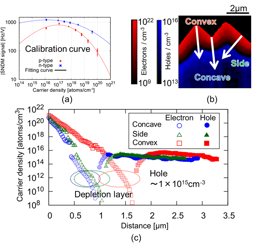
Fig. 13: (a) Calibration curves showing the relationship between SNDM signal strength and carrier density. (b) Carrier density image converted using these calibration curves. (c) Line profiles of carrier distribution.
Super-higher-order SNDM
Recently, a new SNDM method, which measures not only the dC/dV term but also higher-order differentiation terms, has been developed. Using this method, we can obtain much more precise physical information of materials and devices. We name this technique super-higher-order scanning nonlinear dielectric microscopy (SHO-SNDM). We can easily reconstruct the C-V curve at each pixel with this method. As a result, the analysis capability is drastically improved. Basically, SHO-SNDM uses the same setup as that of conventional SNDM except for the use of multichannel lock-in amplifier. When SHO-SNDM measurement is performed, we detect higher-harmonic components, as illustrated in Fig.14, differently from conventional SNDM measurement, which detects the first-order harmonic component dC/dV only. The oscillating frequency deviation Δf(t) is proportional to the tip-sample capacitance variation ΔCs(t), which is modulated as a function of the applied ac voltage V(t)=Vpcosωst between the tip and the sample. The relationship between Δf(t)and ΔCs(t) is given by
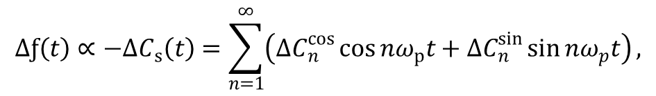
where Cncos and Cnsin are the Fourier coefficients. Thus, ΔCncos and ΔCnsin are obtained by extracting the n-th order harmonic component in ΔCs(t), which is proportional to a demodulated FM signal of the SNDM probe. ΔCnsin directly correlates with the delay in the capacitance response to the applied voltage, so ΔCnsin=0 indicates no delay. The C-V curve is reconstructed from a combination of ΔCs(t), which is calculated from ΔCncos and ΔCnsin, and V(t) using time t as a parameter. The obtained C-V curve is not affected by slow minority-carrier generation because a relatively high frequency ac bias voltage is applied. Measurement of the higher-order differentiation term is equivalent to detection of each harmonics of Fourier series expansion, so that SHO-SNDM is very useful for solving several problems in semiconductor evaluation and characterization.
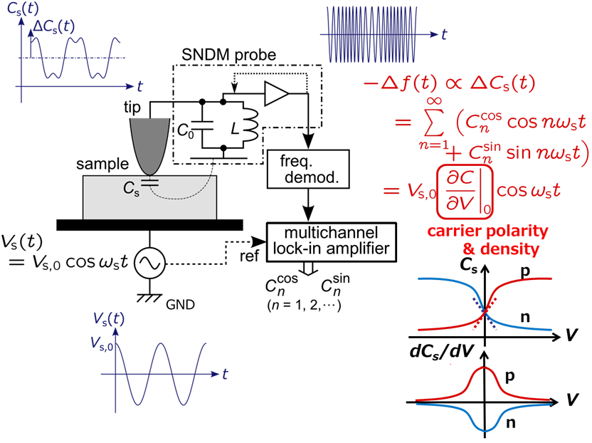
Fig. 14: Schematic diagram of scanning nonlinear dielectric microscopy and super-higher-order-scanning nonlinear dielectric microscopy.
Depletion layer distribution analysis based on the shape of the reconstructed C-V curve is possible. The C–V curve is obtained by plotting [Cs(t), V(t)] on the V–Cs plane at various t in the range of -π/ωp and +π/ωp. C-V curves with monotonic increase and decrease are obtained when the tip is on the p- and n-type areas, respectively. When the tip is on the depletion layer, a V-shaped C-V curve is expected since the capacitance under the tip is affected by the type of carrier (p- or n-type). We consider the situation where the tip is on the depletion region. When the bias V becomes negative, electrons from the n-type region approach the tip, which increases in Cs. When V becomes positive, Cs also increases since holes from the p-type region approach the tip. Therefore, in the depletion region, a V-shaped C-V curve is obtained. This effect reflects a contribution to the tip-sample capacitance from both the p- and n-type regions. To demonstrate the above analysis, we measured a cross-sectional SiC-MOSFET using SHO-SNDM. Figure 15 shows two-dimensional distributions of up to the sixth harmonic component. Figure 16 shows typical C-V curves (reconstructed at each pixel) and the result of visualization of the depletion layer. As mentioned above, from the shape of the C-V curve at each pixel, we can judge the type of the pixel, i.e., p-type, n-type, and depletion layer (p-type, monotonic increase; n-type, monotonic decrease; depletion layer, V-shaped). Then, the distribution of the depletion layer was clearly visualized. As described above, it is clearly shown that SHO-SNDM is very effective for the visualization of the depletion layer in semiconductor devices and carrier distribution in operated devices.
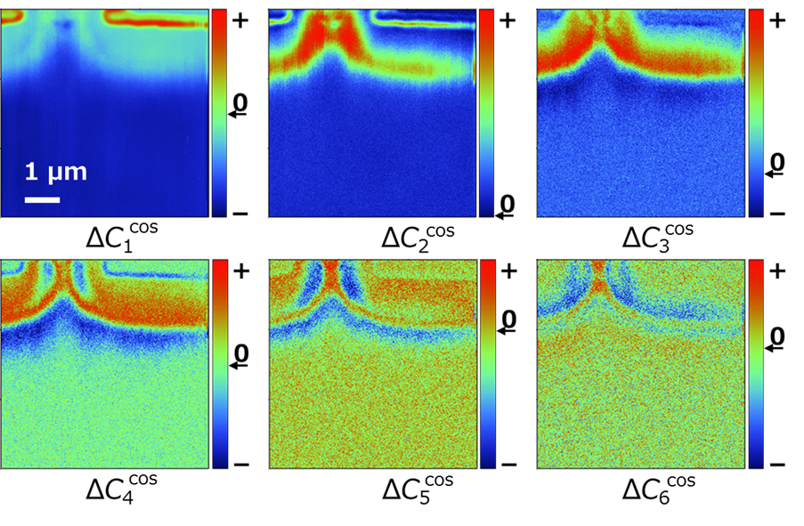
Fig. 15: Acquired images of ΔCncos (n=1,2,…….,6).
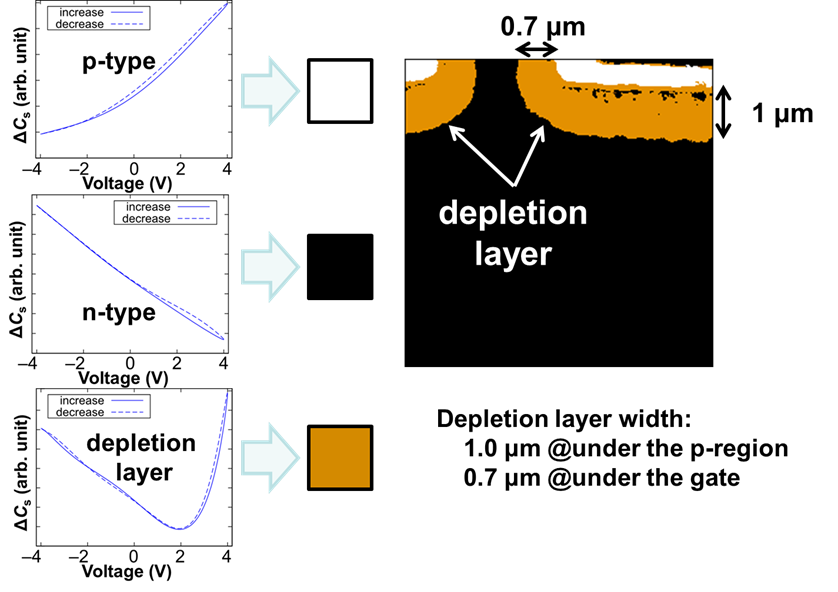
Fig. 16: Typical C-V curves and the result of visualization of depletion layer.
Local-deep-level transient spectroscopy for investigation of MOS interface traps
Physical properties of the metal-oxide-semiconductor (MOS) interface are critical for semiconductor devices. There are several techniques of characterizing MOS interface properties. Deep level transient spectroscopy (DLTS) is one of powerful techniques capable of macroscopic quantitative evaluation of trap density at/near the MOS interface (Dit). However, it can be easily imagined that actual traps are not homogeneously distributed but have two-dimensional distributions in the atomic scale and even in the mesoscopic scale. Therefore, it is very important to characterize the MOS interface microscopically. Unfortunately, it is impossible to observe such inhomogeneity by conventional macroscopic DLTS methods. Moreover, to the best of our knowledge, scanning probe microscopy-based two-dimensional DLTS imaging has not been reported. Here, a new technique for local DLTS imaging based on SHO-SNDM is proposed. This method enables us to observe the two-dimensional distribution of trap density at/near the MOS interface and is demonstrated with oxidized SiC wafers. In local-DLTS measurement, the conductive sharp tip comes in contact with the surface of SiO2/SiC sample, which forms a tiny MOS capacitor whose capacitance Cs is modulated by external pulse voltage application. The voltage waveform applied to a sample is shown in Fig. 17(a); the dc bias and filling pulse bias with a duration of tpw are Va and Vb, respectively. The voltage-induced capacitance variation ΔCs(t) is measured through the modulation of the oscillating frequency of a free-running GHz-range LC oscillator (SNDM probe). The samples investigated here are as follows. 45-nm-thick thermal oxide layers were formed on three Si-faces of 4°-off n-type 4H-SiC wafers. One of them was labeled #S-45-1. The other two wafers were subjected to post-oxidation annealing (POA) in nitric oxide (NO) under different conditions as follows: 1250 °C for 10 min (#S-45-2), and 1150 °C for 60 min (#S-45-3). The average Dit values of these samples were preliminarily measured by a conventional macroscopic high-low method, which showed that the Dit of #S-45-1 was highest and that of #S-45-3 was lowest. These three samples were scanned on a 1.5x1.5 µm2 square area with a resolution of 30x30 pixels and analyzed using the proposed local-DLTS method By analyzing the acquired images, the time constant τ and the magnitude of transient capacitance response were obtained at each pixel. Figure 18 shows images of local-DLTS signals at approximately \tau;=1µs. The highest brightness was obtained from #S-45-1 and the lowest one from #S-45-3, which is consistent with the macroscopically obtained result. Furthermore, in the local-DLTS images, we detected dark and bright areas, which indicate the two-dimensional trap distribution.
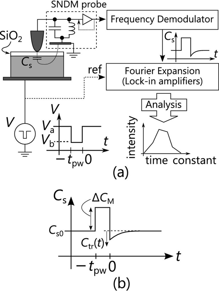
Fig. 17: Principle of local-DLTS. (a) Block diagram of the measurement system, where free-running LC oscillator with conductive sharp tip (SNDM probe) is used for detection of capacitance variation under the tip induced by voltage pulse with pulse duration of tpw applied between tip and sample. (b) Ideal curve of capacitance response to voltage pulse.
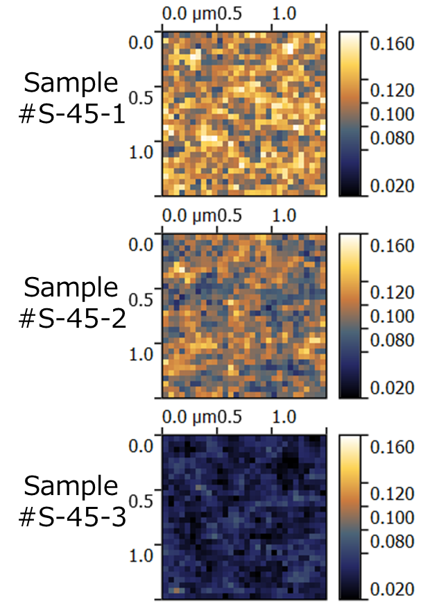
Fig. 18: Images of local-DLTS signals at approximately t=1µs in SiC MOS interface. The dark and bright areas indicate low-Dit (trap density) area and high-Dit area, respectively.
Time-resolved SNDM (Tr-SNDM)
The time-resolved measurement of capacitance is a powerful experimental technique used for the characterization of defects in semiconductors. We demonstrated time-resolved capacitance measurements at the nanoscale using scanning nonlinear dielectric microscopy (SNDM). We detected the capacitance transient of SiO2/4H-SiC interfaces triggered by the application of a 3-ns pulse, which showed the high temporal resolution of the method developed. We characterized the density and activation energy of defects at SiO2/4H-SiC interfaces, which verified the quantitative capability and high sensitivity of the method. Two-dimensional mapping of the interface states showed nanoscale inhomogeneous contrasts, suggesting that the physical origins of defects at SiO2/4H-SiC interfaces are microscopically clustered. Moreover, high-resolution observation of the density of interface states (Dit) at SiO2/4H-SiC interfaces was performed by local deep-level transient spectroscopy (DLTS) based on time-resolved SNDM (tr-SNDM). The non-uniform contrasts observed in the Dit map were several tens of nanometers in size. Simulation of the tr-SNDM measurement suggested that the spatial resolution of tr-SNDM is roughly equal to the tip radius of the cantilever used for the measurement and can be smaller than the lateral spread of the depletion layer width.
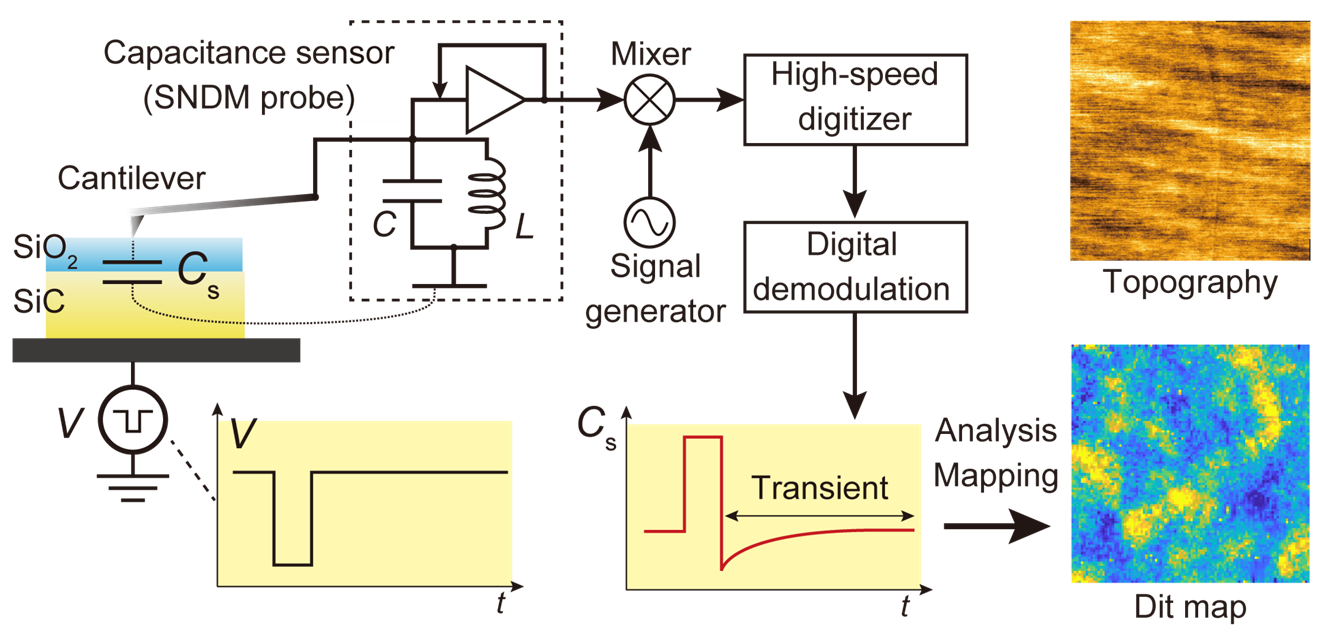
Fig. 19: Schematic of tr-SNDM measurement setup.
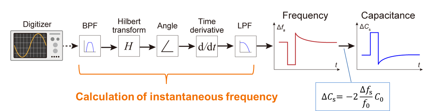
Fig. 20: Calculation procedure for instantaneous frequency using Hilbert transform in Tr-SNDM.
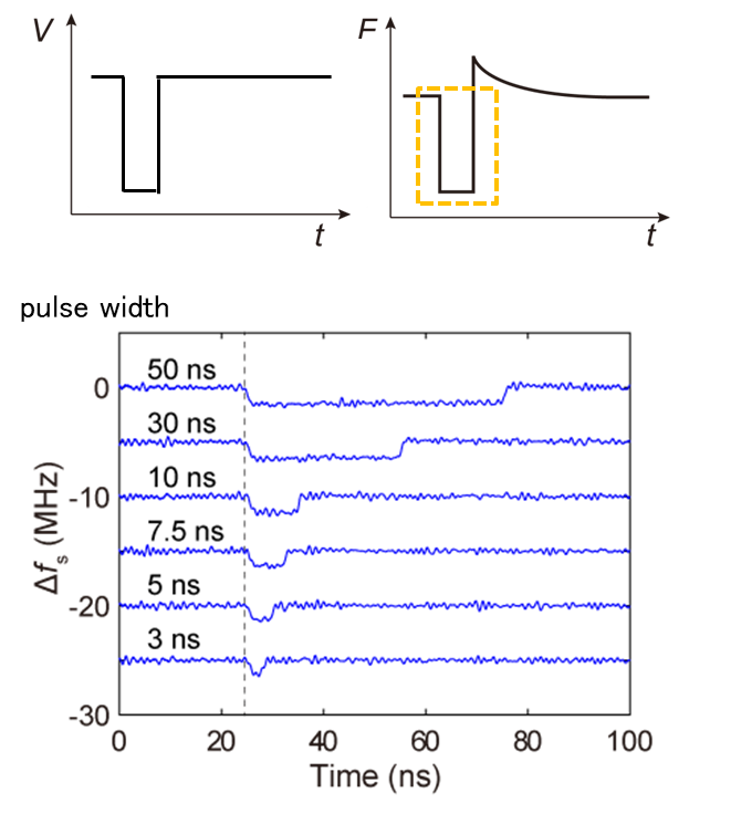
Fig. 21: Time evolution of Δfs measured as a function of pulse width. Sample voltage was tuned from +10 to -10 V at t = 25 ns. Each waveform is displaced along the vertical axis at 5-MHz intervals.
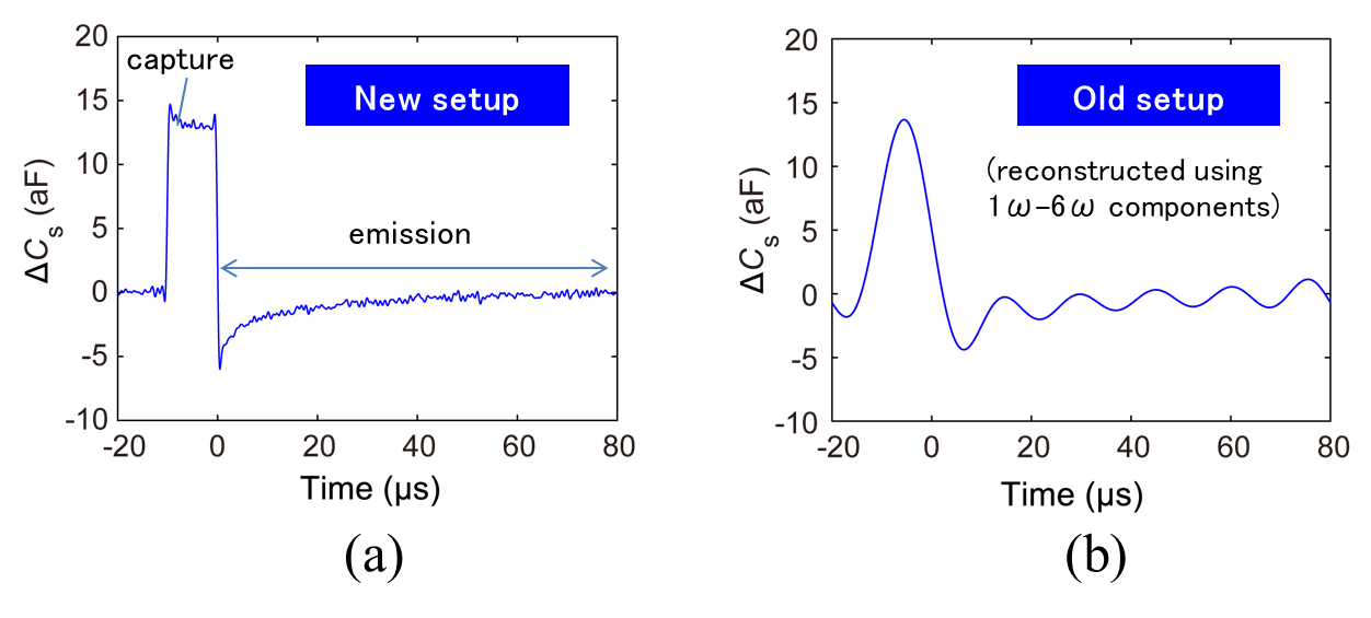
Fig. 23: Comparison of capacitance waveforms. Time evolutions of ΔCs measured under an applied voltage pulse with a width of 10 µs (Va and Vb were set to +2 and -8 V, respectively) for a SiO2/SiC sample, acquired by using (a) the present tr-SNDM-based setup and (b) an old setup using a FM demodulator and multichannel lock-in amplifier.
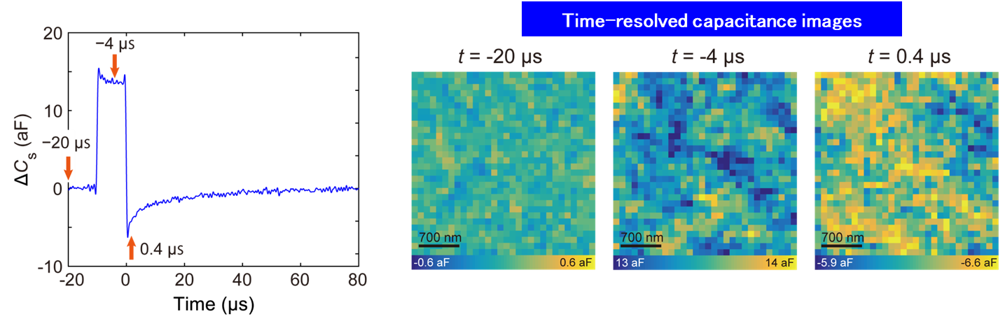
Fig. 24: Reconstructed ΔCs images taken under a voltage pulse with a width of 10 µs applied at t = -10 µs. Note that each image is shown with different color scales to emphasize the inhomogeneous contrasts observed in the images. From left to right, the images correspond to t = -20 µs, t = -4 µs, and t = 0.4 µs.
Nanoscale carrier distribution imaging on atomically-thin (two-dimensional) semiconductors
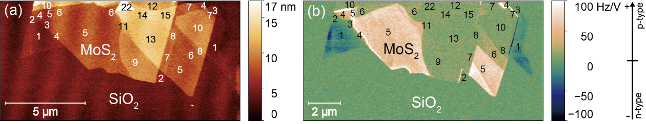
Fig. 25:SNDM imaging of atomically-thin niobium doped MoS2 layers mechanically exfoliated on SiO2. (a) Topographic image (b) SNDM image.Arabic numbers in (a) and (b) indicate the estimated number of stacking MoS2 layers. [Reprinted with permission from Fig. 4, J. Appl. Phys. 128, 074301(2020). Copyright 2020 American Institute of Physics]
In addition to semiconductors such as silicon and silicon carbide, SNDM can also be applied to the nanoscale observation of carrier distribution in atomically-thin layered, or two-dimensional, semiconductors. Recently, atomically-thin layered materials, such as graphene, have been extensively studied because of their unique properties and emerging device applications. Among the layered materials, atomically-thin layered semiconductors that exhibit semiconductor properties such as molybdenum disulfide (MoS2) are expected as next-generation semiconductor materials. The above figure shows a SNDM image of a niobium-doped MoS2 mechanically exfoliated on a thermally oxidized Si substrate. Niobium is doped to make MoS2 to p-type, but it is not always obvious that niobium-doped MoS2 retains its properties as a p-type semiconductor, especially when the material is atomically-thin. In fact, the SNDM image clearly shows that, as expected, p-type majority carriers were detected on the multilayer part, while n-type carriers were unexpectedly detected on the single-layer part that should have also been p-type. In more detail, we found that the concentration of holes had no significant dependence on the number of layers (L) for L more than about 10, but, it began to decrease as L decreased less than about 10, became almost depleted for few-layers, and finally changed to an n-type semiconductor at L=1. In view of the previous studies by other groups, SNDM imaging shows that the effect of niobium doping was reduced by the unintentional donors generated on the surface of MoS2, and as the number of layers became thinner, the surface n-doping from the surface exceeded the effect of niobium p-doping, resulting in overcompensation causing p- to n-type transition. Unlike the existing semiconductors such as silicon, atomically-thin layered semiconductors are very thin and therefore their characteristics are strongly influenced by the properties of their surfaces and interfaces rather than bulk parts. In addition, when the same sample was treated by UV/ozone oxidation, it was found that p- to n-type transition was promoted and, as shown in the figure below, n-type carriers became dominant even on the stacking layers with up to about 5 layers. In the fabrication of devices such as transistors using atomically-thin layered semiconductors, various treatments will be applied to the materials and may give significant impacts on their characteristics. It is thus necessary to evaluate the influence of the treatments such as the changes in dominant carrier concentration. Our results demonstrate that SNDM will be a useful evaluation tool for the fabrication process of devices using atomically-thin layered semiconductors.
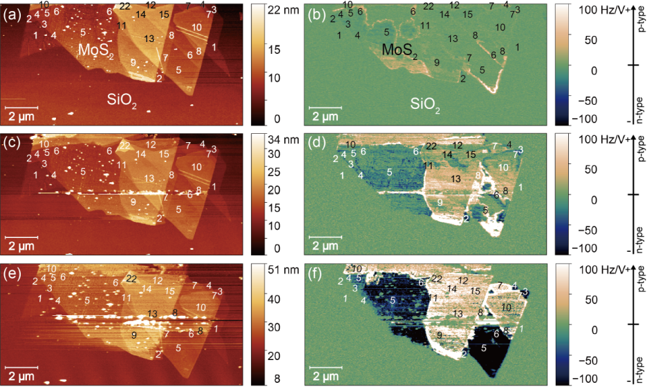
Fig. 26: SNDM images of the UV/ozone treated sample. SNDM images were taken after 10 min. [(a) and (b)], subsequent 5 min. (15 min. total) [(c) and (d)], and extra 5 min. (20 min. total) [(e) and (f)] UV/ozone treatments. The sample was the same as that imaged in the figure above. (a), (c), and (e) show topography and (b), (d) and (f) SNDM images. [Reprinted with permission from Fig. 6, J. Appl. Phys. 128, 074301(2020). Copyright 2020 American Institute of Physics]
Observation of electron and hole distribution in 3D flash memory by SNDM
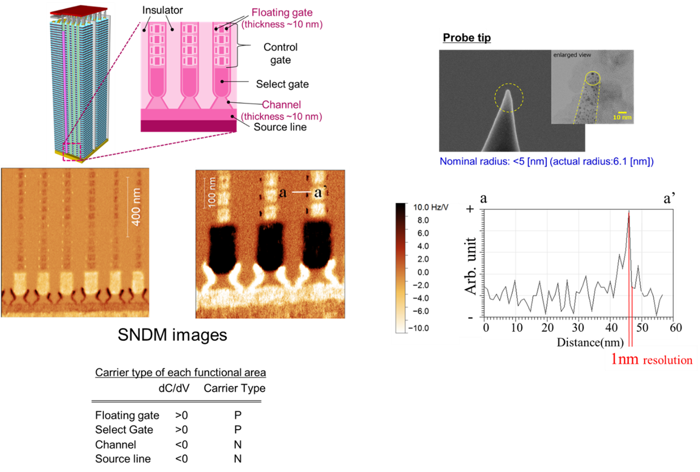
The latest flash memory has a three-dimensional (3D) structure to increase the storage capacity. Here, we introduce the results of clearly measuring the carrier distribution in floating gate and channel structures in 3D flash memory cells smaller than 10 [nm] using a scanning nonlinear dielectric microscopy (SNDM). Using super-sharp diamond tips with radius of <5 nm to achieve the supreme spatial resolution, we successfully obtained SNDM signals of floating gate in high contrast to the background. We deduced the minimum spatial resolution and confirmed that our SNDM exhibits the spatial resolution as good as < 1.9 [nm]. Furthermore, we seized a clear evidence that the diffusion length differences of the n-type impurity among the channels are < 21 [nm]. These mean that we successfully established an exceptionally effective method for the device performance optimization and the device failure analysis.
- K. Honda, K. Ishikawa, and Y. Cho: J.Phys.: Conf. Ser. 209 (2010) 012050
- N. Chinone and Y. Cho: IEEE Transactions on Electron Devices 63 (2016) 3165
- K. Hirose, Y. Goto, N. Chinone, and Y. Cho: Jpn. J. Appl. Phys 55 (2016) 08NB13
- K. Hirose, K. Tanahashi, H. Takato, and Y. Cho: Appl. Phys. Lett. 111 (2017) 032101
- N. Chinone and Y. Cho: J. Appl. Phys. 122 (2017) 105701
- Y. Yamagishi and Y. Cho: Appl. Phys. Lett. 111 (2017) 163103
- K. Yamasue and Y. Cho: Appl. Phys. Lett. 112 (2018) 243102
- J. Hirota, K. Yamasue, and Y. Cho: Microelectronics Reliability 114 (2020) 113774