


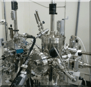
Atomic Resolution Imaging
There are various types of SNDM developed by our group. Among them, noncontact SNDM (NC-SNDM) operated in ultrahigh vacuum has extremely high sensitivity that enables the atomic resolution imaging of polarization distribution, or dipole moment imaging of individual atoms, on cleaned surfaces. In addition, as a potentiometric extension of SNDM, we here introduce scanning nonlinear dielectric potentiometry (SNDP), which can provide quantitative information on spontaneous polarization of surfaces and interfaces.
Principle of noncontact imaging
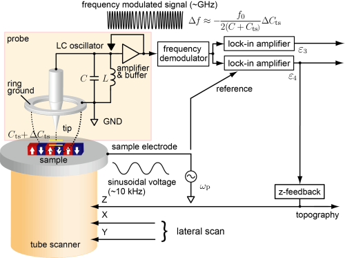
As described in the principle of SNDM, a metal tip needs to scan over a sample surface in order to map the polarization distribution of the surface. The problem here is that the tip apex and surface may be damaged in the original setup of SNDM, because the tip apex contacts with the surface during scan. This is caused by strong contact force between the tip apex and sample surface. In order to avoid the damage and perform stable atomic resolution imaging, a constant tip-sample distance needs to be maintained. How can we keep the tip-sample distance ?
Nonlinear dielectric constants are usable for this purpose as well as imaging polarization distribution. Since nonlinear dielectric constants sensed by the tip depend on the tip-sample distance, the distance can be kept constant if we make a feedback controller maintaining constant nonlinear dielectric constant during scanning the sample surface. ε4, one of the higher order nonlinear dielectric constants, is suitable for feedback signal.
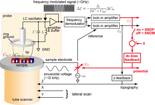
Schematic diagram of NC-SNDM is shown in the next figure. The difference from typical SNDM is that another lock-in amplifier for measuring ε4 and feedback electronics using it is additionally implemented to the setup. The tip-sample distance is kept constant by feedback electronics and also sample topography is reconstructed from the record of control input. As a result, we can simultaneously acquire topography and polarization distribution of sample surfaces without damaging the tip and surfaces.
As you might have noticed, the principle of noncontact operation described above is the same as feedback control used in various types of scanning probe microscopy such as scanning tunneling microscopy (STM) and noncontact atomic force microscopy (NC-AFM). This means that our equipment can be used as STM and NC-AFM as well as NC-SNDM. These operating modes differ in only signal, or physical quantity, used in feedback and, by combining these different operating modes, we can evaluate samples from different physical aspects. We briefly introduce two major results achieved by NC-SNDM below.
Observation of atomic dipole moments on cleaned semiconductor surface
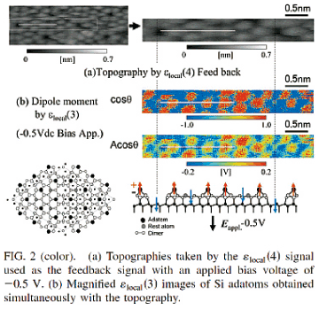
The next figure shows atomic resolution NC-SNDM images of a Si(111)-(7×7) surface [Reprinted with permission from Fig. 2, Phys. Rev. Lett. 99, 186101(2007). Copyright 2007 American Institute of Physics].We can simultaneously image a topographic image acquired from ε4 and polarization distribution from ε3. As shown in the figure, the adatoms on the Si(111)- (7×7) surface have upward (outward pointing normal to surface) dipole moments in the ε3 image. We consider these upward atomic dipole moments are formed by the charge distribution around an individual adatom, which has a positively charged nucleus and triple covalent bonds that connect the nucleus to second-layer atoms. This result demonstrates that NC-SNDM is useful for directly imaging dipole moments of individual adatoms on surfaces.
Observation of atomic dipole moments on cleaned semiconductor surface
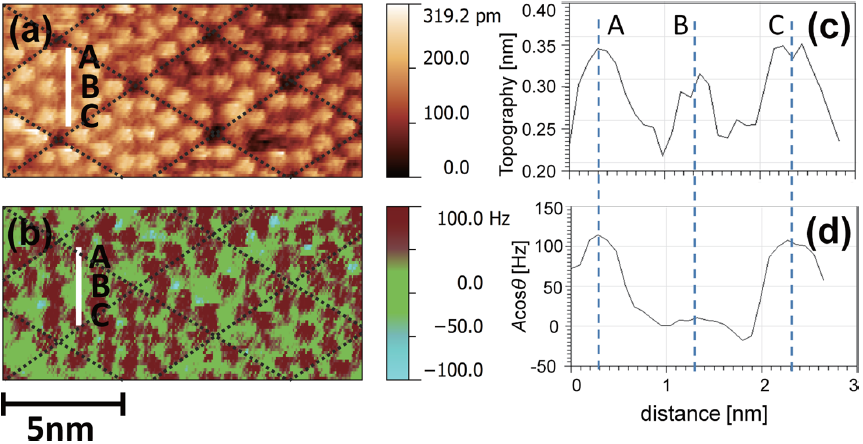
By using NC-SNDM, it is also possible to observe the change of dipole moments due to the adsorption of atoms on a surface. The right figure shows a NC-SNDM image of a Si(111)-(7 × 7) reconstructed surface after the exposure of atomic hydrogen [Reprinted with permission from Fig. 3, Appl. Phys. Lett. 103, 101601 ( 2013). Copyright 2013 American Institute of Physics]. Although the topographic image shown in (a) does not seem to be different from the Si (111)-(7 × 7) structure in the previous section, the dipole moment image shown in (b) partly differs from that for the bare silicon surface. In contrast to the bare silicon adatoms having an upward dipole moment (for example, ε3 > 0 in “A” and “C” in the figure), ε3 signal is almost zero on some of the atoms (for example, “B” in the figure). When the dangling bonds of the bare silicon atoms are terminated by the adsorption of atomic hydrogen, the charge redistribution occurs at an atomic level. The SNDM image suggest that the charge distribution on the terminated silicon atoms become nearly symmetric and then the dipole moments are reduced on these atoms. Our result suggests that silicon adatoms are deactivated both chemically and electrically by hydrogen termination.
Imaging of C60 molecules on Si(111)-(7×7) surface
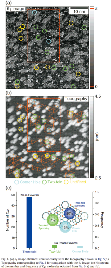
The next figure shows NC-SNDM images of C60 molecules deposited on a Si(111)-(7×7) surface [S. Kobayashi and Y. Cho, Surface Science 606, 174(2012)]. NC-SNDM has successfully achieved simultaneous imaging of topography and polarization distribution. In the topography, we can see many C60 molecules as protrusions with about 1nm height (note that tip-sample convolution makes protrusions appear large). It is also shown that C60 molecules have downward dipole moments on the Si(111)-(7×7) surface. We consider these dipole moments arise from the charge transfer from the adatoms to C60 molecules. On the other hand, we also could notice that some of the C60 molecules did not have downward dipole moments. These molecules are located at sites other than the three-fold symmetry sites on the Si(111)-(7×7) surface.These results show that NC-SNDM has a potential to capture physics on interfaces as well as surfaces.
Atomic resolution imaging of layered semiconductor materials
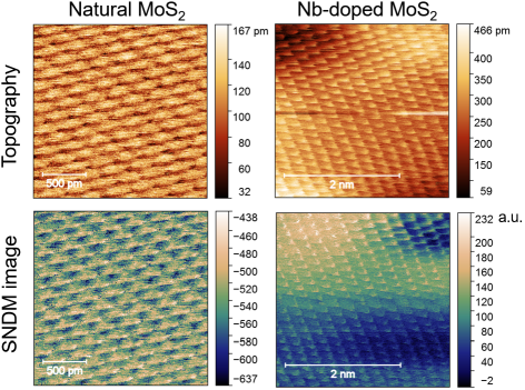
In recent years, layered materials such as transition metal dichalcogenides have attracted attention. In particular, molybdenum disulfide (MoS2) is expected to be a material for next-generation electronic devices owing to its semiconductive properties especially exhibited in the atomically-thin crystals. While the SNDM image reflects the polarization distribution, as described on the Electronic Device Measurement page, the polarity and distribution of semiconductor majority carriers can also be imaged. The figure on the right shows atomic resolution topographic (upper row) and SNDM (lower row) images of an undoped bulk MoS2 crystal (left column), which is usually an n-type semiconductor, and bulky MoS2 (right column) doped with niobium to make it p-type. Basically, the signal polarities on undoped and Nb-doped MoS2 are opposite in the SNDM images, which shows that they have n- and p-type majority carriers, respectively. At the same time, an atomic scale features are obtained on a smaller scale. In this way, NC-SNDM provides images that simultaneously reflect the atomic scale surface structure, charge distribution, and carrier distribution in layered semiconductors.
Development of scanning nonlinear dielectric potentiometry (SNDP)
As already described above, NC-SNDM can determine the polarity of spontaneous polarization on a sample surface through the measurement of a ε3-signal. Here, we introduce a slight modification of NC-SNDM to acquire quantitative information on spontaneous polarization.
In general, as described in the principle of SNDM, a dielectric material is polarized by applying an electric field to it. Here, let us consider that we apply an external voltage to effectively cancel out spontaneous polarization by opposite polarization induced by the voltage. It is shown that, if the cancellation is complete, the applied voltage becomes approximately equivalent to the potential induced by spontaneous polarization. This scheme can be easily implemented to SNDM, because SNDM allows us to measure the voltage compensating spontaneous polarization based on the measurement of the ε3-signal. As shown in figure below, a potential image is acquired from a feedback controlled voltage to cancel out the ε3-signal [Reprinted with permission from Fig. 2, Rev. Sci. Instrum. 86(9), 093704(2015). Copyright 2015 American Institute of Physics]. We named this extension method as scanning nonlinear dielectric potentiometry (SNDP). Non-contact operation (NC-SNDP) is also possible using ε4-feedback and thus a topographic image can be obtained simultaneously.
Note that Kelvin probe force microscopy (KPFM), which is well-known as an extension of AFM, also gives a potential image of a sample surface by cancelling out an electrostatic force between the tip and the surface. The difference is that KPFM is sensitive to contact potential difference (CPD) and fixed surface charges as well as spontaneous polarization. In contrast, SNDP is selectively sensitive to spontaneous polarization. Therefore, SNDP will be an efficient tool for the investigation of spontaneous polarization or permanent dipoles in materials and devices.
NC-SNDP study on interfacial charge states of graphene on SiC
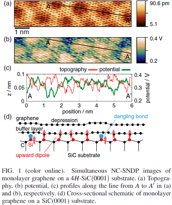
NC-SNDP has been applied to atomic resolution imaging of graphene on SiC, which is a carbon-based two-dimensional material promising for future high speed electronic device applications. The figure on the right shows NC-SNDP images of monolayer graphene on a 4H-SiC(0001) substrate [Reprinted with permission from Fig. 1, Phys. Rev. Lett. 114, 226103 (2015). Copyright 2015 American Institute of Physics]. We simultaneously acquired topographic and potential images. In the topography, we see a honeycomb structure made of the carbon atoms' network of graphene. There is also a super-periodic quasi (6×6) structure arising from a corrugating graphene-SiC interface. The potentials were as high as 0.3-0.4V, which are significantly higher than those on graphite. Since graphene has symmetric charge distribution because of its sp2 configuration, we believe that these high potentials originate from spontaneous polarization on the SiC-graphene interface. NC-SNDP will be useful for investigating the influence of interface on top-layer graphene, whose electronic properties are significantly affected by the interfacial charge states.